Processor Structure and Functions
This article discusses the principles, structures and functions of a microprocessor.
1 Overview
The microprocessor, also known as the CPU(Central Processing Unit) is the controlling unit of a computer fabricated on a integrated circuit capable of performing ALU(Arithmetic Logical Unit) operations and communicating with the other devices connected to it.
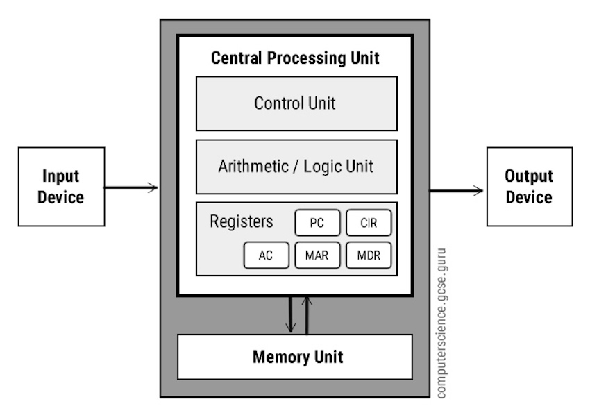
- Microprocessor consists of an ALU, a register array, a control unit as shown in the diagram below:

- This diagram is called the Von Neumann architecture. It is a model developed by John von Neumann, which describes a design architecture for an electronic digital computer.
2 How the microprocessor works?
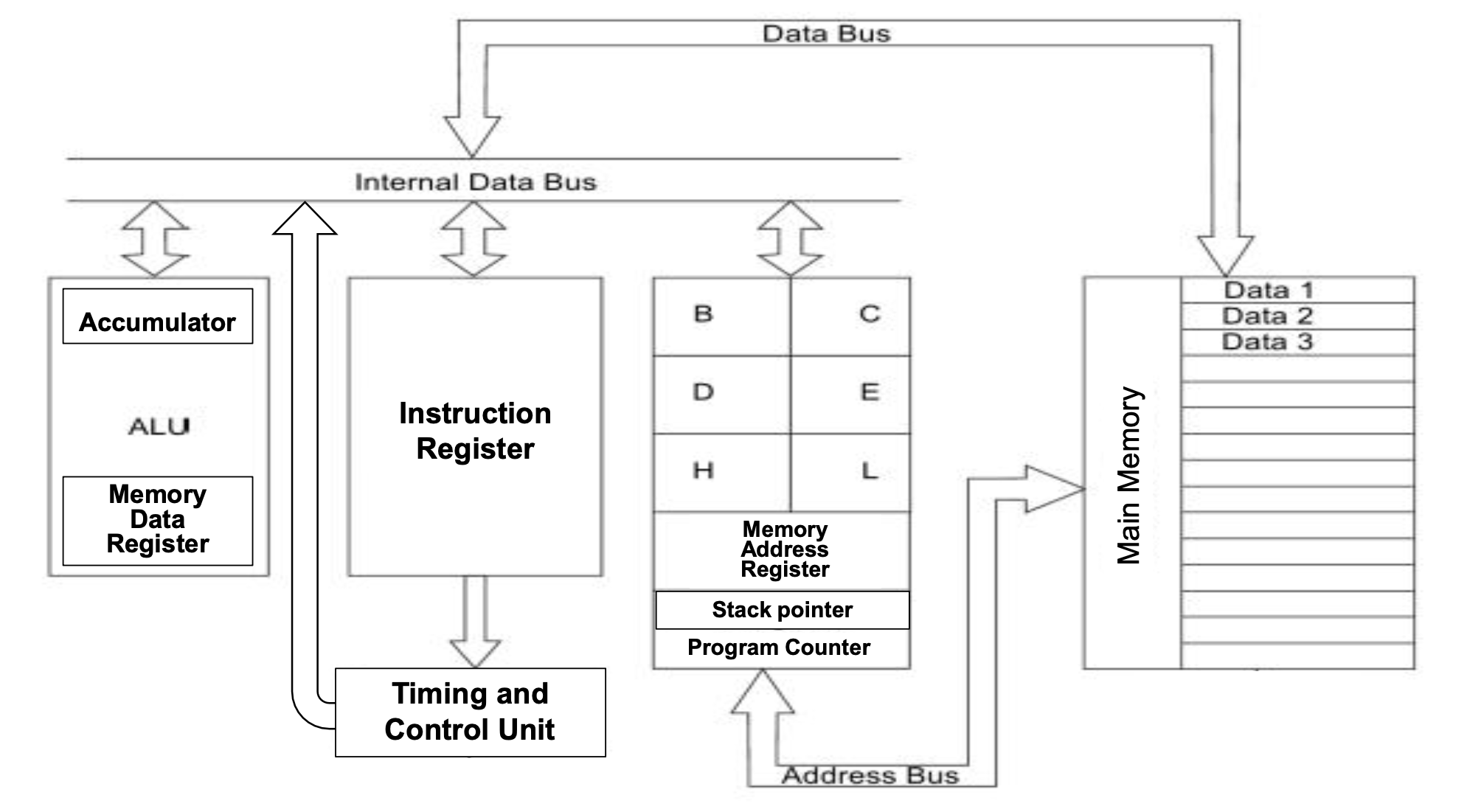
Structure of a 8085 Microprocessor:

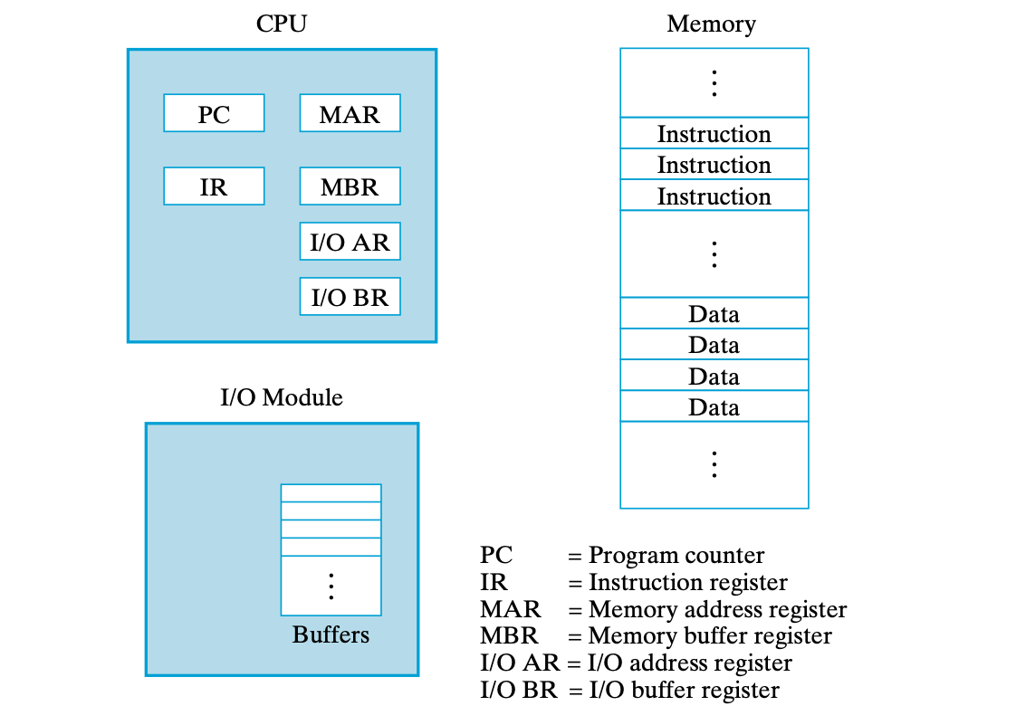
At a top level, a computer consists of processor, memory, and I/O components, with one or more modules of each type.
- Processor: Controls the operation of the computer and performs its data processing functions.
- Main Memory: Stores data and programs. This memory is typically volatile.
- I/O Modules: Move data between the computer and its external environment. The external environment consists of a variety of external devices, including secondary memory devices, communications equipment, and printers.
- System Interconnection: Some structure and mechanisms that provide for communication among processors, main memory, and I/O modules.
2.1 Computer Components

The processor controls operations. One of its functions is to exchange data with memory. For this purpose, it typically makes use of two internal (to the processor) registers:
- a memory address register (MAR), which specifies the address in memory for the next read or write;
- and a memory buffer register (MBR), which contains the data to be written into memory or which receives the data read from memory.
- Similarly, an I/O address register (I/OAR) specifies a particular I/O device.
- An I/O buffer register (I/OBR) is used for the exchange of data between an I/O module and the processor.
A memory module consists of a set of locations, defined by sequentially numbered addresses.
- Each location contains a binary number that can be interpreted as either an instruction or data.
- An I/O module transfers data from external devices to processor and memory, and vice versa. It contains internal buffers for temporarily holding this data until it can be sent on.
2.2 Processor Registers
Within the processor, there is a set of registers that provide a level of memory that is faster and smaller than main memory.
- Registers are a type of computer memory used to quickly accept, store, and transfer data and instructions that are being used immediately by the CPU.
Registers of the 8085 Microprocessor
1. General Purpose Registers
The 8085 has six general-purpose registers to store 8-bit data; these are identified as- B, C, D, E, H, and L. These can be combined as register pairs – BC, DE, and HL, to perform some 16-bit operation. These registers are used to store or copy temporary data, by using instructions, during the execution of the program
2. Special Purpose Registers
(a) Accumulator (AC)
The accumulator is an 8-bit register (can store 8-bit data) that is the part of the arithmetic and logical unit (ALU). After performing arithmetical or logical operations, the result is stored in accumulator.
(b) Flag Registers
The flag register consists of 8 bits and only 5 of them are useful. These 5 flags are set or reset (when value of flag is 1, then it is said to be set and when value is 0, then it is said to be reset) after an operation according to data condition of the result in the accumulator and other registers. The 5 flag registers are:
- Sign Flag (S) - indicates whether the number stored in the accumulator is positive or negative. If the sign flag is set, it means that number stored in the accumulator is negative, and if reset, then the number is positive.
- Zero Flag (Z) - It is set, when the operation performed in the ALU results in zero(all 8 bits are zero), otherwise it is reset. It helps in determining if two numbers are equal or not.
- Auxiliary Carry Flag (AC) - In an arithmetic operation, when a carry flag is generated by the third bit and passed on to the fourth bit, then the Auxiliary Carry flag is set. It is used internally for BCD(Binary-Coded decimal Number) operations.
- Parity Carry Flag (P) - If the accumulator holds even number of 1’s, then this flag is set and it is said to even parity. On the other hand if the number of 1’s is odd, then it is reset and it is said to be odd parity.
- Carry Flag (CY) - If the arithmetic operation results in a carry(if result is more than 8 bit), then Carry Flag is set; otherwise it is reset.
(c) Current Instruction Register (CIR)
The CIR contains the current instruction during processing, so that it can be decoded and input to the control and timing unit.
(d) Program counter (PC)
This register is used to sequence the execution of the instructions. When a byte (machine code) is being fetched, the program counter is incremented by one to point to the next memory location.
(e) Stack Pointer (SP)
The stack is a reserved area of the memory in the RAM where temporary information may be stored. A 16-bit stack pointer is used as a memory pointer. It points to a memory location in the stack. It is always incremented/decremented by 2 during push and pop operation.
(e) Program Status Word (PSW)
The PWS is a an area of memory or a hardware register, which holds a collection of data that are 8 bytes long that reflects the current CPU state. It includes the instruction address, condition code, and other fields.
(f) Memory Address Register (MAR)
It is connected to the address lines of the system bus. It specifies the address in memory for a read or write operation.
(g) Memory Buffer Register (MBR)
It is connected to the data lines of the system bus. It contains the value to be stored in memory or the last value read from the memory.
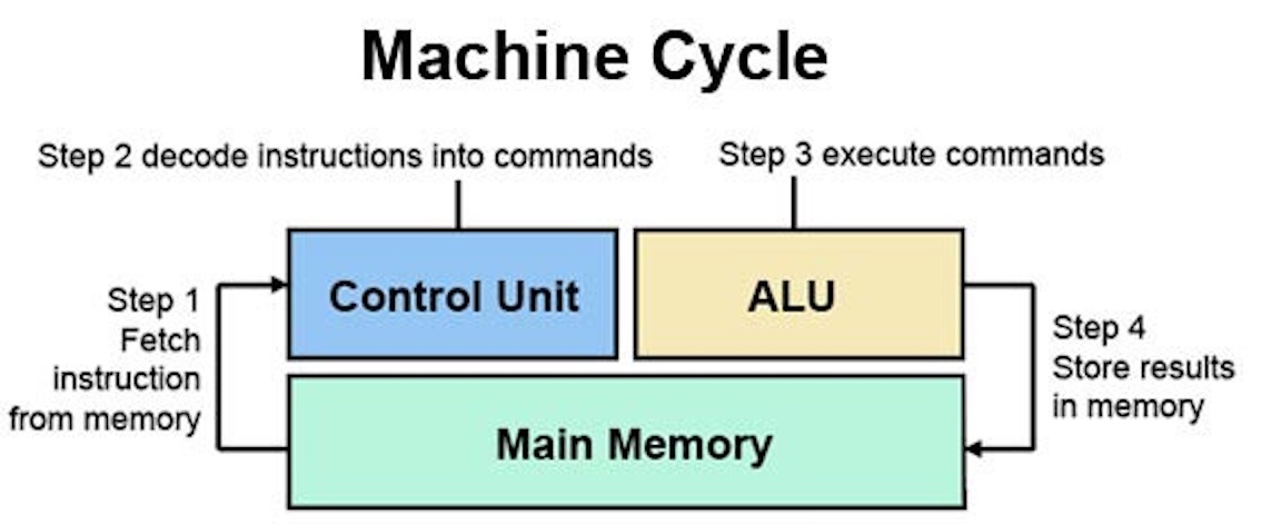
3 Machine Cycle (Fetch, Decode, Execute, Store)

The steps performed by the processor on each instructions received is called the machine cycle. It is a 4 step process that includes reading and interpreting the machine language, executing the code, and then storing that code.
3.1 Control Unit
The control unit directs operations within a computer’s processor. It communicates with both the arithmetic logic unit(ALU) and the main memory.
- The function of a control unit is to generate relevant timing and control signals to all operations in the computer. It instructs the ALU that which logical or arithmetic operation is to be performed.
- It also controls the flow of data between rhe procerssor, memory and peripherals(I/O devices).
3.2 Arithmetic Logic Unit (ALU)
The ALU carries out arithmetic and logic operations on the operands in computer instruction words.
- Typically, the ALU has direct input and output access to the control unit, main memory and I/O devices.
- Inputs and outputs flow along an electronic path that is called a bus.
- The input consists of an instruction word that contains an operation code or “opcode,” one or more operands and sometimes a format code. The operation code tells the ALU what operation to perform and the operands are used in the operation.
- For example, two operands might be added together. The format may be combined with the opcode and tells, for example, whether this is a fixed-point or a floating-point instruction.
3.3 System Bus
A bus is an electrically conducting path along which data is transmitted inside any digital electronic device. A bus which is used to provide communication between the major components of a computer is called a system bus.
System bus contains 3 categories of lines used to provide the communication between the CPU, memory and IO named as:
1. Address Bus
- Used to carry the address to memory and IO.
- Undirectional
- Based on width of a address bus we can determine the capacity of a main memory
2. Data Bus
- Used to carry the binary data between the CPU, memory and IO.
- Bidirectional.
- Based on the width of a data bus we can determine the word length of a CPU, and bsed on the word length we can determine the performance of a CPU.
3. Control Bus
- Used to carry the control signals and timing signals
- Control signals indicates type of operation.
- Timing Signals used to synchronize the memory and IO operations with a CPU clock.
3.4 Main Memory
Main memory refers to physical memory that is internal to the computer. More specifically, main memory is a computer’s short-term storage. It hols data that the CPU needs to access frequently, such as instructions and data currently being processed. On the other hand, auxiliary memory holds data and programs not currently in use and provides long-term storage.
4 Improving the Machine Cycle
Early computer processors needed to wait until an instruction completed all four stages before beginning work on the next instruction. However, today’s computers use pipelining, which allows the processor to begin fetching a second instruction before it has completed the machine cycle for another instruction.
